- 您现在的位置:买卖IC网 > Sheet目录2001 > ISL35822LPIK (Intersil)IC CLOCK/DATA RECOVERY 192EBGA-B
24
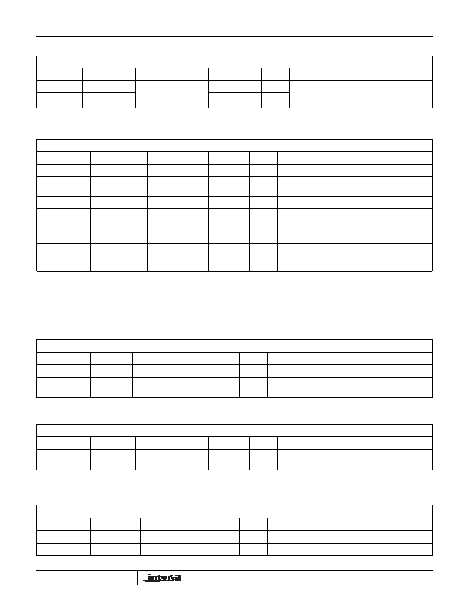
XENPAK-DEFINED REGISTERS (1.8000’H TO 1.8106’H)
Note (1): User writes to these bits are not valid unless the Command Status is Idle. The Command Status will not return to Idle until read after command completion
(either Succeed or Failed).
Note (2): At the end of a hardware RESET via the RSTN pin, on powerup, or on a register [1,3,4].0.15 RESET operation, and if the XP_ENA pin is asserted, the
ISL35822 will automatically begin an ‘all NVR read’ operation.
Note (3): The single byte commands are controlled through the bits of the registers at 1.32769:32774 (1.8001:8006’h). The ‘block write/read’ commands are affected by
register 1.32773 (1.8005’h). Additional status is available in 1.327743 (1.8006’h)
Note (1): 8-bit-addressed I2C devices are addressed using bits 7:0. Never set bit 1.32773.8 (1.8005’h.8) for 16-bit address operation with an 8-bit address I2C device.
Table 14. IEEE PACKAGE IDENTIFIER REGISTERS
MDIO REGISTER ADDRESSES = 1.14:15 (1.000E:F’h)
BIT
NAME
SETTING
DEFAULT
R/W
DESCRIPTION
1.14.15:0
Package ID
Package OUI bits 3:24 &
etc.
00’h
R/W
If NVR is loaded, these are copies of
1.32818:32819 (1.8032:8033’h) & 1.32820:32821
(1.8034:8035’h)
1.15.15:0
Package ID
00’h
R/W
Table 15. XENPAK NVR CONTROL & STATUS REGISTER
MDIO (XENPAK) REGISTER ADDRESS = 1.32768 (1.8000’h)
BIT
NAME
SETTING
DEFAULT
R/W
DESCRIPTION
1.32768.15:6
Reserved
000’h
R/W
1.32768.5
NVR Command(1)
1 = Write NVR
0 = Read NVR
0’b(2)
R/W
Write/Read Control for I2C operation
1.32768.4
Reserved
0’b
RO
1.32768.3:2
NVR Command
Status(3)
Current Status of
NVR Command
00’b
RO
11 = Command failed
10 = Command in progress/Queued
01 = Command completed with success
00 = Idle
1.32768.1:0
Extended NVR
Command
NVR operation to be
performed
11’b(2)
R/W
10 = read/write one byte(3)
11 = read/write all NVR contents(3)
Other values = reserved
Table 16. I2C ONE-BYTE OPERATION DEVICE ADDRESS REGISTER
MDIO REGISTER ADDRESS = 1.32769 (1.8001’h)
BIT
NAME
SETTING
DEFAULT
R/W
DESCRIPTION
1.32769.15:8
Reserved
00’h
RO
1.32769.7:0
Device
Address
I2C Device address to
access
A2’h
R/W
All I2C Device addresses are even. Bit 0 cannot be set.
Table 17. I2C ONE-BYTE OPERATION MEMORY ADDRESS REGISTER
MDIO REGISTER, ADDRESS = 1.32770 (1.8002’h)
BIT
NAME
SETTING
DEFAULT
R/W
DESCRIPTION
1.32770.15:0
Memory
Address
I2C Memory address to
access
0000’h(2)
R/W
I2C Memory Address within Device address of 1.32769
(1.8001’h)
Table 18. I2C ONE-BYTE OPERATION READ DATA REGISTER
MDIO REGISTER ADDRESS = 1.32771 (1.8003’h)
BIT
NAME
SETTING
DEFAULT
R/W
DESCRIPTION
1.32771.15:8
Reserved
00’h
RO
1.32771.7:0
Read Data
I2C Read Data
00’h
RO
Result of I2C 1-byte Read operation
ISL35822
发布紧急采购,3分钟左右您将得到回复。
相关PDF资料
ISL41334IRZ-T7A
IC TXRX RS232/485 DL 2PRT 40QFN
ISL43485IB-T
IC TXRX 1TX/1RX 3V RS-485 8-SOIC
ISL51002CQZ-110
IC FRONT END 10BIT VID 128-MQFP
ISL5314IN
IC SYNTHESIZER DIGITAL 48-MQFP
ISL55100AIRZ-T
IC COMP DRVR/WINDOW 18V 72-QFN
ISL55100BIRZ
IC COMP DRVR/WINDOW 18V 72-QFN
ISL5627INZ
IC DAC DUAL 8BIT 3.3V 48-LQFP
ISL5629/2INZ
IC DAC 8BIT CMOS DUAL 48LQFP
相关代理商/技术参数
ISL36111
制造商:INTERSIL 制造商全称:Intersil Corporation 功能描述:11.1Gb/s Lane Extender
ISL36111DRZ-EVALZ
功能描述:EVAL BOARD FOR ISL36111DRZ RoHS:是 类别:编程器,开发系统 >> 评估演示板和套件 系列:* 产品培训模块:Obsolescence Mitigation Program 标准包装:1 系列:- 主要目的:电源管理,电池充电器 嵌入式:否 已用 IC / 零件:MAX8903A 主要属性:1 芯锂离子电池 次要属性:状态 LED 已供物品:板
ISL36111DRZ-T7
功能描述:IC EQUALIZER REC 11.1GBPS 16QFN RoHS:是 类别:集成电路 (IC) >> 接口 - 专用 系列:QLx™ 特色产品:NXP - I2C Interface 标准包装:1 系列:- 应用:2 通道 I²C 多路复用器 接口:I²C,SM 总线 电源电压:2.3 V ~ 5.5 V 封装/外壳:16-TSSOP(0.173",4.40mm 宽) 供应商设备封装:16-TSSOP 包装:剪切带 (CT) 安装类型:表面贴装 产品目录页面:825 (CN2011-ZH PDF) 其它名称:568-1854-1
ISL36111DRZ-TS
功能描述:IC EQUALIZER REC 11.1GBPS 16QFN RoHS:是 类别:集成电路 (IC) >> 接口 - 专用 系列:QLx™ 标准包装:3,000 系列:- 应用:PDA,便携式音频/视频,智能电话 接口:I²C,2 线串口 电源电压:1.65 V ~ 3.6 V 封装/外壳:24-WQFN 裸露焊盘 供应商设备封装:24-QFN 裸露焊盘(4x4) 包装:带卷 (TR) 安装类型:表面贴装 产品目录页面:1015 (CN2011-ZH PDF) 其它名称:296-25223-2
ISL36356A-APDK
制造商:INTERSIL 制造商全称:Intersil Corporation 功能描述:PRISM 11Mbps Wireless Local Area Network Access Point
ISL36356A-APDK-EVAL
制造商:INTERSIL 制造商全称:Intersil Corporation 功能描述:PRISM 11Mbps Wireless Local Area Network Access Point
ISL36411
制造商:INTERSIL 制造商全称:Intersil Corporation 功能描述:Quad Lane Extender
ISL36411DRZ-EVALZ
功能描述:EVAL BOARD FOR ISL36411DRZ RoHS:是 类别:编程器,开发系统 >> 评估演示板和套件 系列:* 产品培训模块:Obsolescence Mitigation Program 标准包装:1 系列:- 主要目的:电源管理,电池充电器 嵌入式:否 已用 IC / 零件:MAX8903A 主要属性:1 芯锂离子电池 次要属性:状态 LED 已供物品:板